

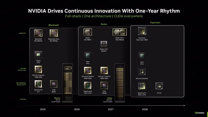
Nvidia is getting ready to vary the foundations of physics in computing. The upcoming “Feynman” GPU structure isn’t simply an improve; it’s a structural revolution that includes 3D stacking and Groq’s LPU expertise.
The way forward for synthetic intelligence is shifting from “studying” to “doing,” and Nvidia’s {hardware} roadmap is adapting to this actuality. New particulars have emerged in regards to the firm’s post-2028 structure, codenamed Feynman, which guarantees to combine Groq’s Language Processing Unit (LPU) expertise instantly into the GPU utilizing superior 3D stacking strategies.
The Hybrid Future: GPU Meets LPU
In keeping with latest leaks and insights from GPU skilled AGF, Nvidia is exploring a design philosophy just like AMD’s X3D expertise however for AI inference. The plan entails stacking LPU items—devoted chips for language processing—instantly on high of the primary GPU die utilizing TSMC’s SoIC hybrid bonding expertise.
This transfer addresses a crucial bottleneck in trendy chip manufacturing: SRAM scaling.
The Drawback: Integrating huge quantities of SRAM (reminiscence) instantly into the primary processor die is changing into inefficient and dear at superior nodes like 1.6nm (A16).The Answer: By separating the LPU and its massive SRAM cache into a definite layer and stacking it vertically, Nvidia can maximize efficiency whereas preserving power consumption low. This enables the primary “Feynman” compute die to be manufactured on the cutting-edge A16 course of, whereas the memory-heavy LPU layer handles the high-speed information entry required for AI brokers.
Engineering Challenges: Warmth and Software program

This formidable leap shouldn’t be with out its dangers. Stacking highly effective compute items creates a major thermal problem. LPUs function with a relentless, high-throughput workload, producing immense warmth that would throttle your complete system if not managed accurately.
Moreover, there’s a software program hurdle. Nvidia’s dominance is constructed on CUDA, a software program ecosystem designed for {hardware} abstraction. LPUs, nonetheless, usually require express reminiscence administration. Merging these two conflicting philosophies would require Nvidia to rewrite the rulebook on how software program talks to {hardware}.
🧠 Metaverse Planet Perspective: Why This Issues?
As we analyze this growth, it’s clear that Nvidia is getting ready for the “Age of Inference.”
For the previous decade, the main focus has been on coaching huge AI fashions (like GPT-4). However sooner or later (2028 and past), the main focus will shift to working billions of AI brokers concurrently in real-time. That’s the place the Feynman structure is available in.
The “Considering” Chip: By integrating Groq’s LPU expertise, Nvidia isn’t simply making a sooner calculator; they’re constructing a chip designed to “communicate” and “perceive” natively. That is the {hardware} required for the true Human 2.0 expertise—the place your AI assistant responds immediately, with zero latency.Past Moore’s Legislation: The shift to 3D stacking proves that we’re reaching the bodily limits of conventional 2D chips. The long run is vertical. Nvidia is actually constructing skyscrapers on silicon to suit the intelligence of the longer term right into a tiny sq..
Backside Line: The Nvidia Feynman is not only a graphics card; it’s the potential engine of the Metaverse, designed to energy a world the place each object and digital entity has its personal intelligence.
